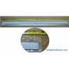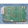
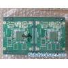

1). 80 *190mm/2up, FR-42). 6 layers at 1.4mm thick3). 35 μm copper weight4). Green solder mask LPI/White legend5). ENIG surface finish6). Blind via from Layer 1 to layer 27). Via in pad plugged conductive resin
|
联系方式
加关注0
BICHENG ENTERPRISE COMPANYVIP会员第13年
资料未认证
保证金未缴纳
|
||||||||||||||||||||||||
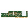
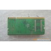
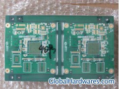
1). 80 *190mm/2up, FR-42). 6 layers at 1.4mm thick3). 35 μm copper weight4). Green solder mask LPI/White legend5). ENIG surface finish6). Blind via from Layer 1 to layer 27). Via in pad plugged conductive resin