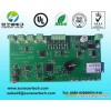

PCB Process Capability *processing layers:1-28 layers*Finished thickness (thinnest - the thickest): 0.008 "~ 0.24" (0.20mm ~ 6.0mm)*Minimum aperture: 6mil (0.15mm)*Minimum line width / spacing :3-4 mil (0.076-0.10mm)*Maximum board size: Single & Double 22 "x 43" (550 x1100mm), Multi-layer 22 "x 25" (550mm x 640mm)*Impedance Control: ± 10%*Surface Treatment: OSP, HASL, Electric Nickel / Gold, Chemical nickel / gold, lead-free HASL , Gold finger, immersion Silver, Immersion Tin.*Base materials: FR4 ( ShengYi, KB, International), high TG (TG150, TG170), halogen-free board (Halogen-free), high frequency plate (Rogers, Teflon, Taconic), made PTFE (PTFE) ,, AL aluminum plate (Berquist, Al-made basis), copper (Cu Base), Iron (Fe Base), ceramic substrate (Ceramic Base)2.Detailed Terms for Pcb Assembly Technical requirement: 1) Professional Surface-mounting and Through-hole soldering Technology2) Various sizes like 1206,0805,0603 components SMT technology3) ICT(In Circuit Test),FCT(Functional Circuit Test) technology.4) PCB Assembly With UL,CE,FCC,Rohs Approval5) Nitrogen gas reflow soldering technology for SMT.6) High Standard SMT&Solder Assembly Line7) High density interconnected board placement technology capacity. Quote requirement:1)Gerber file and Bom list2)Clear pictures of pcb/ fpc/ pcba or pcba sample for us3)The PCB specification: Copper thickness(18um or 35um?); Finished board thickness(0.8mm or 1.6mm?); Surface treatment(lead-free HASL or immersion gold?)4)Test method for PCB/PCBAPS:If you have not Gerber file,plz sent the 1~2 pieces pcb/pcba samples to us,if your pcb have any special demand, pls note clearly in your enquiry,this is necessary. Only this we can quote to you at first time.